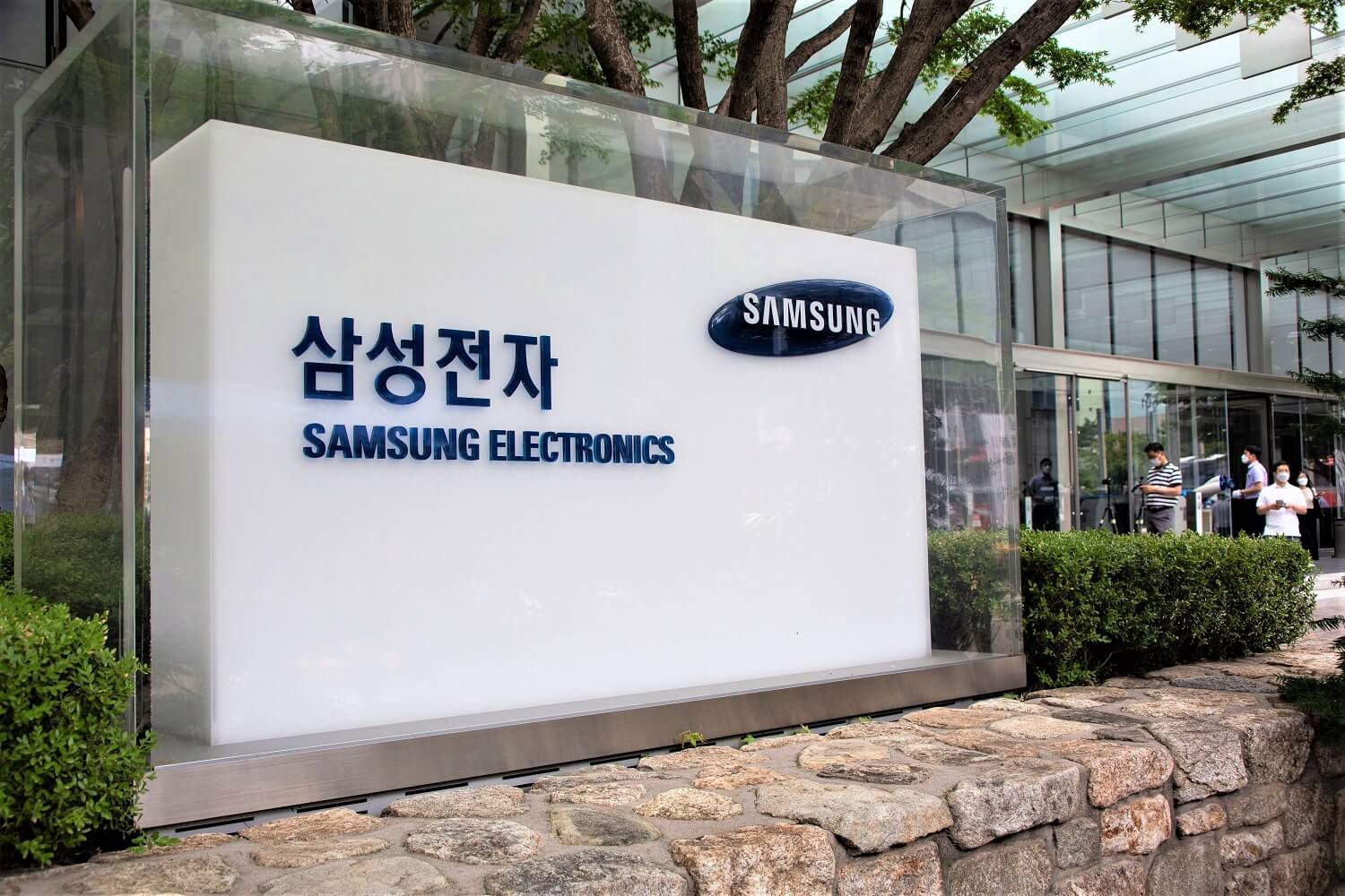
According to THEELEC, Samsung Display and its parent company Samsung Electronics are evaluating the potential use of its LCD factory in Cheonan, South Korea, which may be transformed into a semiconductor factory.
The factory was built in 1996 and covers an area of approximately 500,000 square meters. The factory has two buildings, L3/L4 and L5/L6, which are mainly used to produce small and medium-sized LCD panels. The A1 production line in this factory is Samsung's first OLED production line, and currently only part of it is running the production of automotive OLED panels. In addition, the factory also has an LCD color filter production line and Samsung SDI's small battery production line.
The report stated that the factory costs tens of millions of dollars in maintenance fees and taxes each year. Although the factory has a low operating rate, Samsung has not sold it because they can transform it into a semiconductor factory.
The report pointed out that the factory can accommodate two 300 mm wafer production lines. L5/L6 are specially designed for processing the 6th generation (1500x1800mm) display panel substrates, with enough space to accommodate 300mm wafer equipment. However, Samsung’s working survey showed that the building will need additional construction to add in earthquake resistance design and other upgrades.
The report also stated that transforming the factory into a semiconductor factory was just one of many options Samsung considered for the Cheonan factory. However, this may be the most profitable option in an environment where global wafer foundry capacity is in short supply.





All Comments (0)