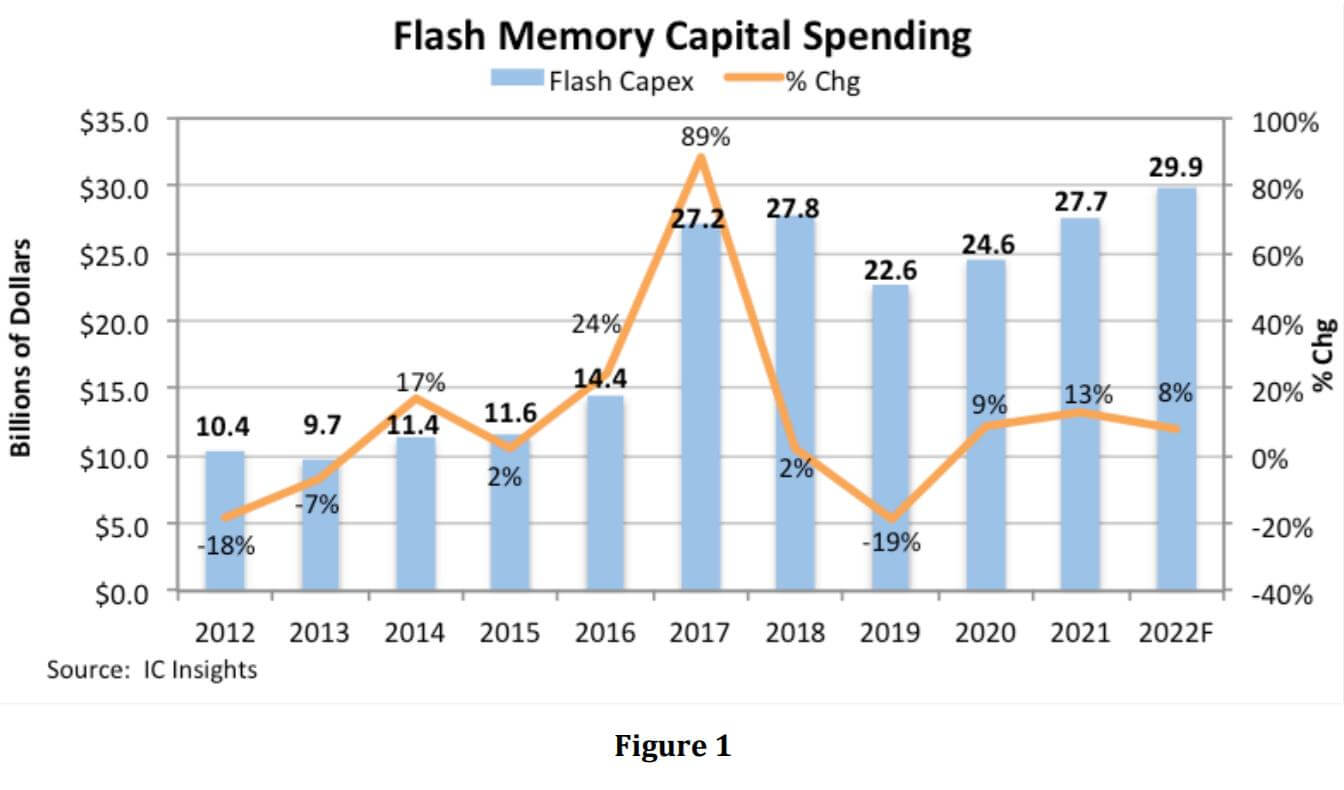
According to a report released by IC Insights, NAND flash capital spending is expected to grow 8% this year to $29.9 billion, surpassing the previous alltime high mark of $27.8 billion spent in 2018 (Figure 1). Flash memory capital spending soared in 2017 when the industry transitioned to 3D NAND and has topped $20.0 billion every year since. In 2022, capital spending for flash memory is forecast to increase to $29.9 billion as big suppliers and small maintain moderately aggressive spending levels another year.
IC Insight stated that the $29.9 billion in spending represents 16% of the $190.4 billion in capital spending forecast for the total IC industry in 2022 and trails only the foundry segment, which is forecast to account for 41% of industry capex this year.
New and recently upgraded NAND flash memory fabs include Samsung’s Pyeongtaek Lines 1 and 2 (which are also used for DRAM and foundry); Samsung’s Phase 2 investment in Xi’an, China; Kioxia’s Fab 6 (Flash Ventures) and Fab K1 in Iwate, Japan; and Micron’s third flash memory plant in Singapore. Also, SK Hynix outfitted the remaining space in its M15 plant for NAND flash.
IC Insights pointed out that through the forecast period, new fabs and new equipment will be needed as NAND flash suppliers gear up to enter the race for 200-plus layer devices starting at the end of 2022 and into 2023. Samsung and Micron might be the first to start volume production of 200-layer devices later this year. Both companies, and SK Hynix, are currently in volume production of 176-layer NAND. Samsung’s wafer fab in Xi’an, China, is (and will be) a key manufacturing location for leading edge NAND with two fabs—each capable of 120,000 wafer starts/month when they are fully operational. With an increased focus on enterprise storage applications, SK Hynix expects to migrate to 196-layers in 2023.






All Comments (0)