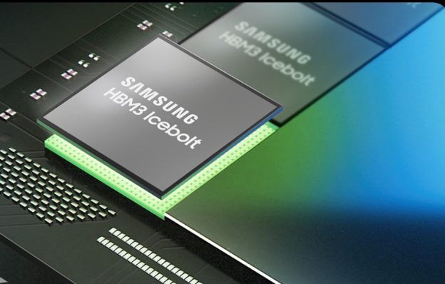
November 13, 2024 /SemiMedia/ — Samsung Electronics announced plans to expand its semiconductor packaging facilities in South Chungcheong Province, South Korea, aiming to increase high-bandwidth memory (HBM) output with a new facility expected to be completed by 2027.
The company will work with the provincial government to transform an idle LCD factory owned by Samsung Display in Cheonan into a semiconductor production site. The Cheonan city and provincial authorities have committed to providing administrative and financial support to ensure smooth project execution.
Scheduled for completion in December 2027, the new plant will feature advanced HBM chip packaging lines. HBM chips are crucial for artificial intelligence (AI) computing, where demand remains strong. Packaging is a key stage in chip manufacturing, providing protection against mechanical and chemical damage.
The upgraded Cheonan plant is expected to help Samsung strengthen its competitiveness in the global semiconductor market, where it has lagged behind major competitor SK Hynix in the HBM sector.
Samsung previously faced delays in supplying its fifth-generation HBM3E products to NVIDIA due to quality concerns. However, Jaejune Kim, Executive Vice President of Samsung’s memory business, noted during a recent earnings call that the company anticipates shipping HBM3E chips to customers in the fourth quarter, having made “meaningful” progress in certification with major clients.






All Comments (0)