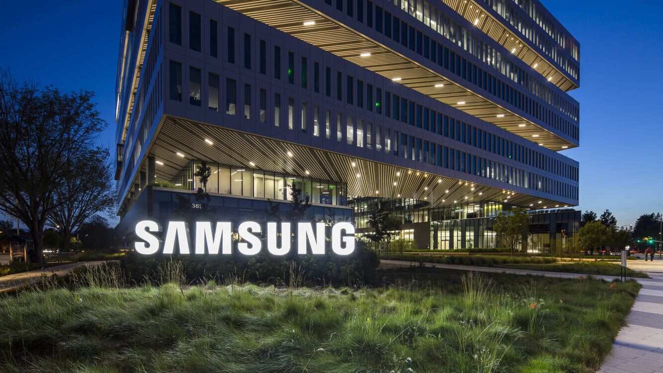
November 20, 2024 /SemiMedia/ — Samsung Electronics announced on November 18 that it held an equipment installation ceremony for its next-generation semiconductor research and development (R&D) complex, NRD-K, located in Giheung, Yongin, South Korea. The facility is slated to begin full-scale operations by mid-2025, with a total investment of 20 trillion won by 2030.
Spanning 109,000 square meters, NRD-K will focus on foundational research and product development across memory, logic, and foundry semiconductor technologies. The complex will house cutting-edge equipment, including high-resolution extreme ultraviolet (EUV) lithography systems, advanced material deposition tools, and wafer bonding infrastructure to enable next-generation memory and innovative semiconductor structures.
Giheung is recognized as the birthplace of Samsung's semiconductor business and a symbol of its global leadership in the memory market, having developed the world's first 64Mb DRAM in 1992. Samsung aims to transform Giheung into a hub for advanced semiconductor ecosystems by leveraging NRD-K as a focal point for collaboration with local materials, components, and equipment suppliers.
“With NRD-K, we will establish a seamless system from fundamental research to mass production for next-generation semiconductor technologies, significantly accelerating our development timeline,” said Jeon Young-hyun, a senior executive in Samsung’s Device Solutions (DS) division. “At Giheung, the starting point of our 50-year semiconductor history, we are laying the foundation for the next 100 years of innovation.”
The equipment installation marks a critical step in Samsung’s drive to secure its position in future semiconductor technologies.





All Comments (0)