
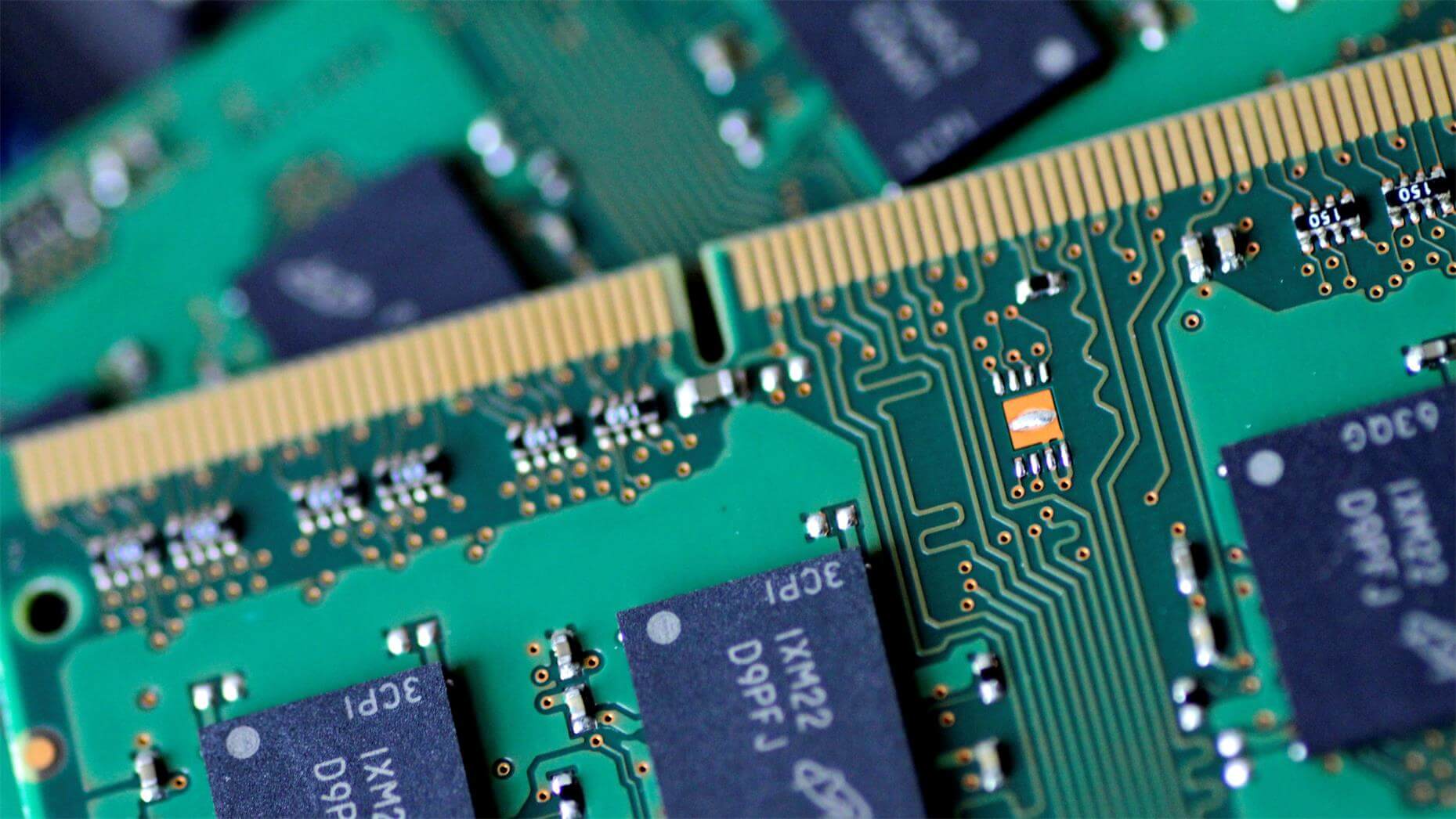
February 24, 2025 /SemiMedia/ — Kioxia, a leading Japanese semiconductor manufacturer, has unveiled its latest innovation in NAND flash memory technology, featuring 332 layers and a 33% boost in interface speed. This new development is expected to meet the increasing demand from artificial intelligence (AI) data centers.
The 10th-generation 332-layer NAND technology offers a 59% improvement in data storage density compared to the previous 8th-generation 218-layer technology. Kioxia, in collaboration with its U.S. partner Sandisk, also highlighted that the new flash memory consumes less power, with data input efficiency improving by 10% and output efficiency increasing by 34%.
While the production of the new flash memory will take place in Japan, Kioxia has not yet disclosed a specific release timeline. The company is joining the ranks of its competitors, who are also developing NAND flash memory technologies with over 300 layers.
Despite the performance benefits of NAND flash memory, such as increased performance through stacked storage cells, rising device costs remain a challenge. Kioxia is also exploring methods to separately manufacture wafers with storage cells and controllers (which manage read/write operations), before bonding them together for more efficient production.
Additionally, Kioxia is working on its 9th-generation flash memory, combining existing storage cell technologies with new innovations to further enhance read/write performance.


All Comments (0)