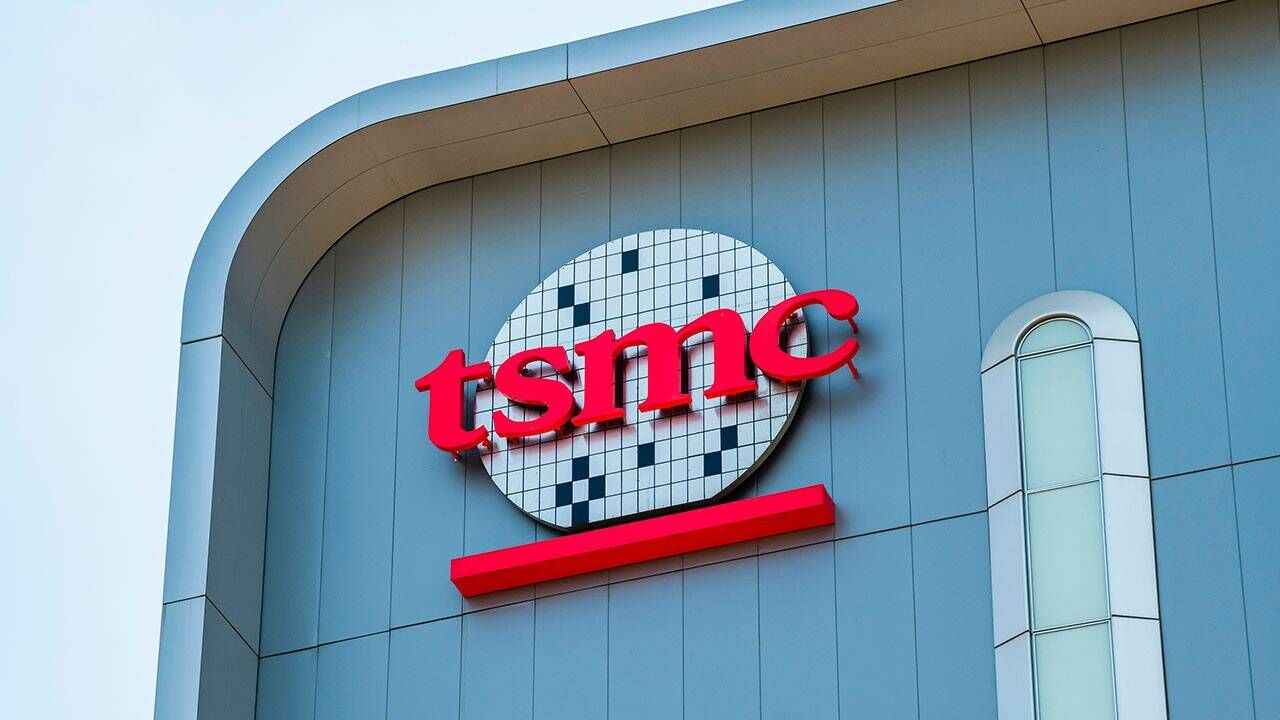
April 18, 2025 /SemiMedia/ — Taiwan Semiconductor Manufacturing Co (TSMC) said on Wednesday it plans to shift approximately 30% of its 2-nanometer and below chip production capacity to the United States, as part of its massive investment in Arizona.
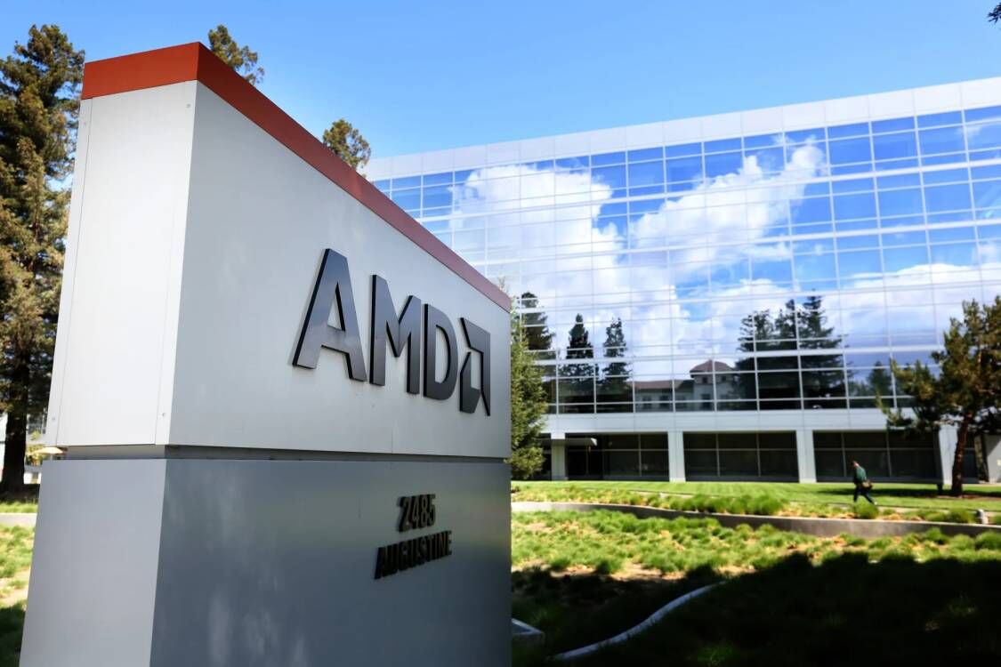
Chairman and CEO C.C. Wei revealed the plan during TSMC’s Q1 earnings call, stating that the advanced capacity will be supported by three Gigafabs under construction in Arizona. The move signals a strategic shift in TSMC’s global manufacturing footprint, driven by rising demand from U.S.-based customers such as Apple, Nvidia, AMD, Qualcomm, and Broadcom.
Wei emphasized that this capacity shift is more than geographic diversification — it reflects a deliberate effort to localize high-end chip production closer to end-market demand and build a robust U.S. semiconductor supply chain. “With 30% of our most advanced nodes in Arizona, we are creating a self-sufficient leading-edge manufacturing cluster,” he said.
The U.S. fabs are expected to play a critical role in serving AI and high-performance computing (HPC) applications, areas where next-generation process nodes are essential. TSMC's advanced packaging and logic technologies are also expected to be integrated locally to support complete platform solutions.
The initiative is part of TSMC’s $100 billion multi-year investment in global expansion, with Arizona emerging as the core site for U.S. production. The company believes the plan will enhance economies of scale, operational resilience, and closer technical alignment with key clients.
While commenting on potential trade and tariff uncertainties, Wei noted that the company remains focused on operational fundamentals and expressed confidence in achieving foundry growth beyond “Foundry 2.0” benchmarks in 2025.


All Comments (0)