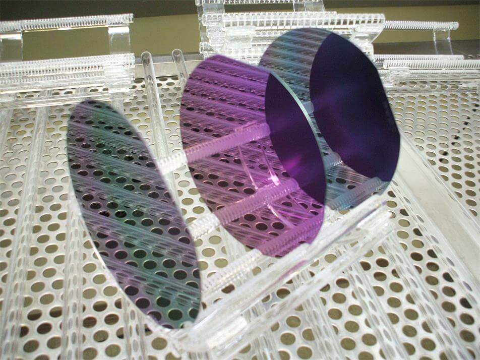
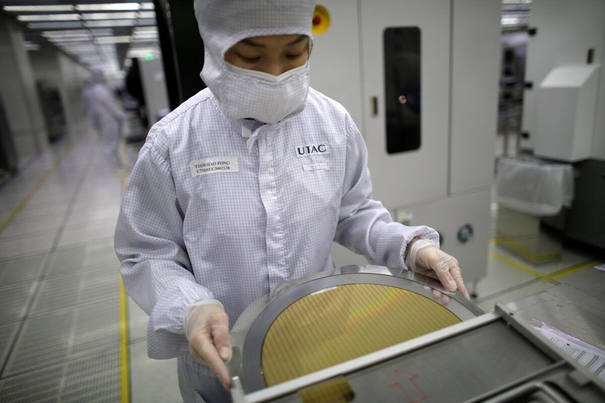
Recently, IC Insights released the global wafer capacity report for 2019-2023. According to the report, as semiconductor industry M&A activity increases, more and more companies are adopting processes below 20nm, forcing more and more manufacturers to phase out inefficient fabs.

According to the above chart, in the past ten years (2009-2018), global semiconductor manufacturers have closed or rebuilt 97 fabs. It includes 42 150mm fabs and 24 200mm fabs. The number of 300mm fabs closed is only 10% of the total.
Of the closed 300mm fabs, two belong to Renesas. Renesas closed a factory in Kochi Prefecture, Japan, which produces analog, logic and some old micro-components. In addition, Renesas has also adjusted its factory in Otsu, Shiga Prefecture, Japan to produce optoelectronic devices.
In the future, as the cost of building new fabs and manufacturing equipment rises, more and more inefficient fabs will be shut down in the future, and more and more IC companies will be transformed into fabs or Fabless.
In addition, IC Insights pointed out five wafer fabs that will be shut down or rebuilt. Samsung's 300mm memory factory (line 13) will be converted into an image sensor production line this year; TI is expected to close its 200mm analog GFAB plant in Greenock, Scotland in June 2019; Renesas expects to close two 150mm fabs in 2020 or 2021; ADI also plans to close its 150mm fab in Milpitas, Calif., in February 2021.

Since 2009, Japan has closed 36 fabs, far more than other countries and regions. In the same period, 31 wafer fabs were closed in North America, 18 fabs were closed in Europe, and 12 were closed in the entire Asia Pacific region (excluding Japan). In Japan, because of the closure of these 36 factories, and almost no new factories have been put into production, it is not surprising that Japan’s semiconductor capital expenditures have become lower and lower in recent years, accounting for only 5% of the world!


All Comments (0)