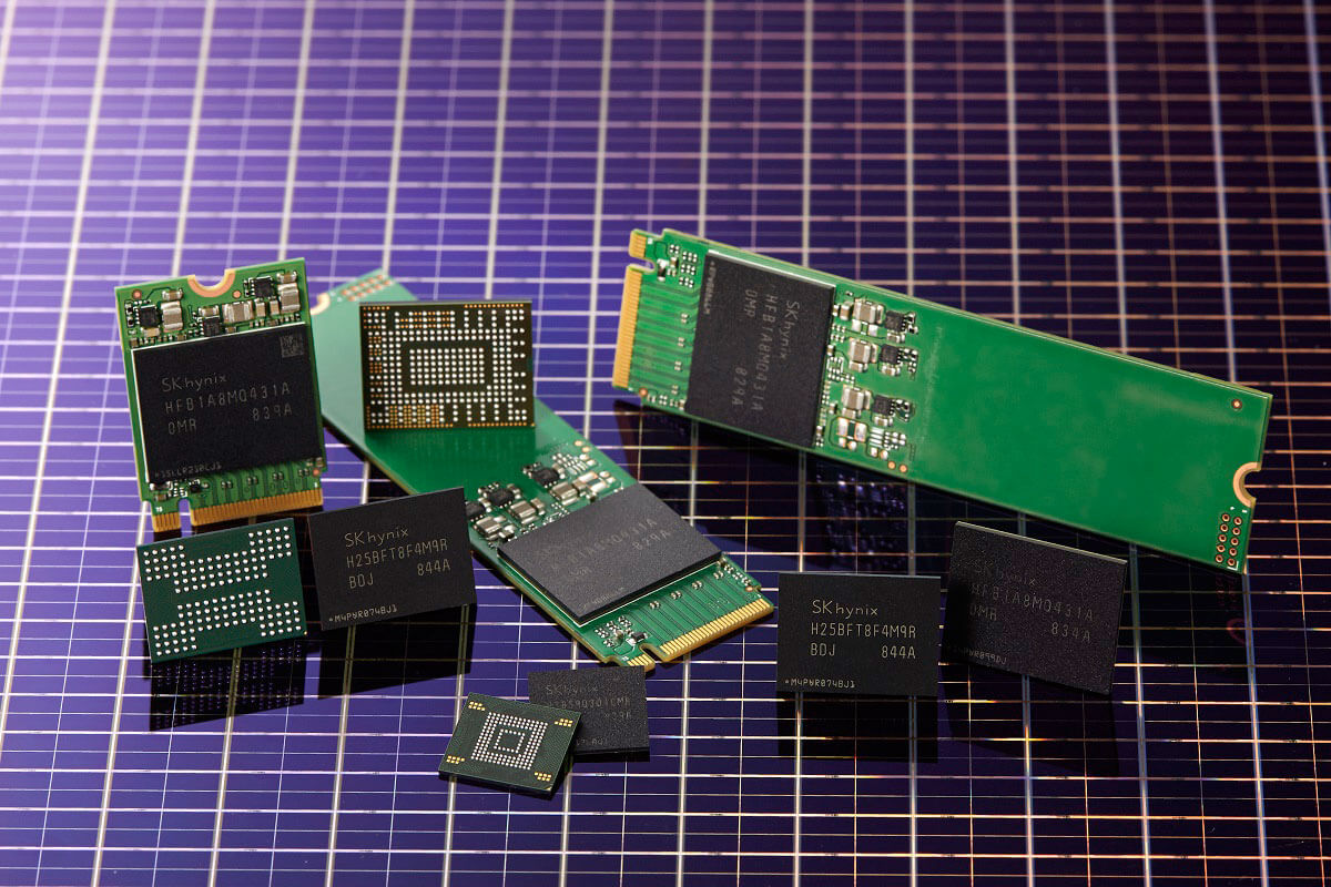
SK hynix announced on the 26th that it will mass produce the world's first 128-layer 1Tb TLC 4D NAND flash memory, and plans to start sales in the second half of the year.
According to Korean media reports, in order to use TLC to design and develop new products, SK hynix uses vertical etching, multi-layer film particle formation, low power loop design and other technologies to produce a stack of more than 360 billion NAND particles and 128 layers of 1Tb products. The product not only reaches the highest stack count in the industry, but also surpasses the 90-layer NAND of Samsung Electronics.
Although there are 96 layers of QLC 1Tb products on the market, TLC's performance and processing speed are better than QLC. In the NAND market, TLC products have a market share of 85%. Therefore, the industry pays special attention to this high-capacity NAND developed by SK hynix with TLC technology.
In particular, although the product adds 32 layers of 96-layer NAND products, the process procedure is reduced by 5%, and the 128-layer 4D NAND has a 40-bit higher productivity per wafer than the 96-layer 4D NAND. Even without PUC technology (Peri Under Cell), the bit productivity of 128-layer 4D NAND can be increased by more than 15%. According to SK hynix, this method can save the cost of converting the new process, which can be reduced by 60% compared with the previous generation conversion investment cost.
About the 128-layer 4D NAND flash memory that SK hynix plans to sell in the second half of the year. According to SK hynix, the product can reach 1400Mbps data transmission speed even in low voltage (1.2V) environment, suitable for high performance, low power consumption mobile solutions, and enterprise SSD.






All Comments (0)