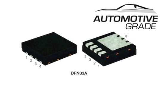
Diodes Incorporated recently announced the introduction of its new family of automotive-compliant clock buffers, designed for low power operation in ambient temperatures of up to 105°C, as found in advanced driver-assistance systems (ADAS), infotainment applications, and automotive gateways.
Increasing sophistication of automotive electronics has led to more complex system clock trees. The increased number of clock signals has created a demand for clock buffers that can deliver low jitter and low skew, while minimizing system power.
Implemented using a low-power CMOS process, the clock buffer family operates from an input voltage of between 1.5V and 3.3V. All clock inputs are aligned and synchronized, which maintains low skew, and the CMOS design introduces minimal phase noise, resulting in very low additive jitter.
The family includes the PI6C49CB01Q (one differential input, one singleended output), PI6C49CB02Q (one single-ended input, two single-ended outputs), and PI6C49CB04xQ (one single-ended input, four single-ended outputs). All inputs and outputs are compatible with LVCMOS/LVTTL signal levels. The parts are qualified to AECQ-100 with full PPAP support and they are manufactured in IATF16949 certified facilities.
More information please visit Diodes’ Clock Buffers page.


All Comments (0)