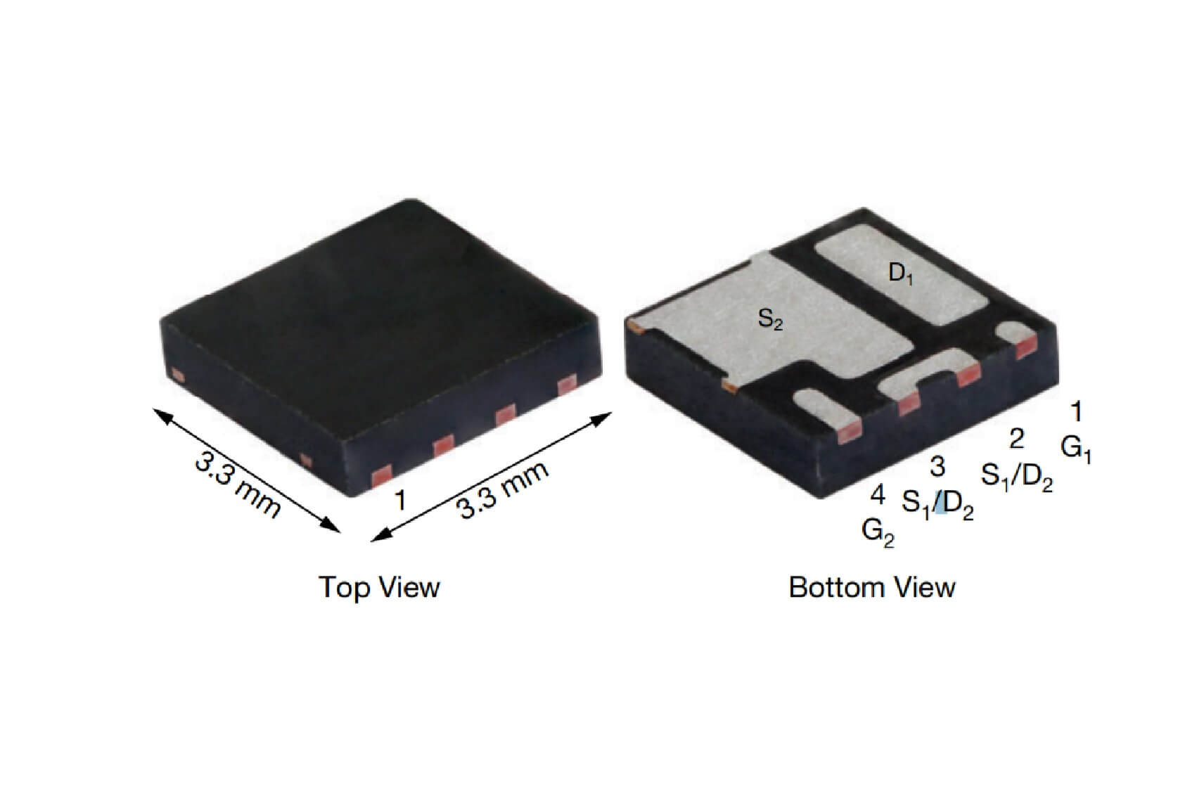
Vishay recently introduced a new 30 V n-channel MOSFET half-bridge power stage that combines a high side TrenchFET® MOSFET and low side SkyFET® MOSFET with integrated Schottky diode in one compact PowerPAIR® 3.3 mm by 3.3 mm package. For power conversion in computing and telecom applications, the Vishay Siliconix SiZF300DT delivers increased power density and efficiency, while reducing component counts and simplifying designs.
The two MOSFETs in the device released today are internally connected in a half-bridge configuration. The Channel 1 MOSFET provides maximum on-resistance of 4.5 mΩ at 10 V and 7.0 mΩ at 4.5 V. The Channel 2 MOSFET features on-resistance of 1.84 mΩ at 10 V and 2.57 mΩ at 4.5 V. Typical gate charge for the MOSFETs is 6.9 nC and 19.4 nC, respectively.
The SiZF300DT is 65 % smaller than dual devices in 6 mm by 5 mm packages with similar on-resistance, making it one of the most compact integrated products on the market. The device provides designers with a space-saving solution for point-of-load (POL) conversion, power supplies and synchronous buck and DC/DC converters in graphic and accelerator cards, computers, servers, and telecom and RF networking equipment.
The dual MOSFET features a unique pin configuration and construction that delivers up to 11 % higher output current per current phase than competing products in the same footprint area, in addition to higher efficiency for output current above 20 A. The device’s pin configuration and large PGND pad also enhance thermal transfer, optimize the electrical path, and enable a simplified PCB layout.
The SiZF300DTis 100 % Rg- and UIS-tested, RoHS-compliant, and halogen-free.
Samples and production quantities of the new dual MOSFET are available now, with lead times of 12 weeks for large orders. More information on this device, please visit: http://www.vishay.com/ppg?76288.


All Comments (0)