ON Semiconductor Corporation announced on 8th it is exploring a sale of its manufacturing facility in Niigata, Japan. The intended sale of Niigata facility is part of the company’s plan to optimize its manufacturing footprint and sharpen its focus on highly differentiated power, analog and sensor products. The company will begin searching for strategic buyers to enter into a mutually beneficial arrangement that is expected to facilitate an orderly transition of products from its facility in Niigata to other facilities in its network.
The Niigata facility is an automotive qualified facility, which meets the IATF 16949 global industry standard for quality management. The company believes that the facility is an attractive semiconductor manufacturing asset. The site is run by a highly skilled and productive workforce capable of managing a large mix of technologies.
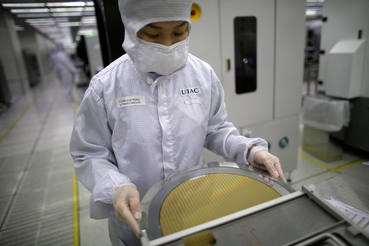
The Niigata facility consists of two co-located wafer fabs with 215,000 square feet of clean room space, located on a 40 acre campus with 1.1 million square feet of building space. The large campus, existing infrastructure and capability of eight inch wafer manufacturing provide potential buyers a compelling growth opportunity. Currently, the facility supports the company’s BCD, BiCMOS, CMOS, Discrete and Smart Discrete technologies.
ON Semiconductor remains committed to growing its presence in Japan, and the company recently added a large eight-inch wafer fab in Aizu to its manufacturing footprint. ON Semiconductor plans to continue to invest in its various functional groups, such as field service, research and development, solution engineering centers, and manufacturing plants to better serve its customers in Japan.








All Comments (0)