SemiMedia SemiMedia
  • Breaking News
  • MarketWatch
  • Distribution
  • Manufacturer
  • Video
  • About us
Home › MarketWatch › ASE's K13 IC packaging & testing plant breaks ground
  • 0

ASE's K13 IC packaging & testing plant breaks ground

SemiMediaEdit
August 17, 2020

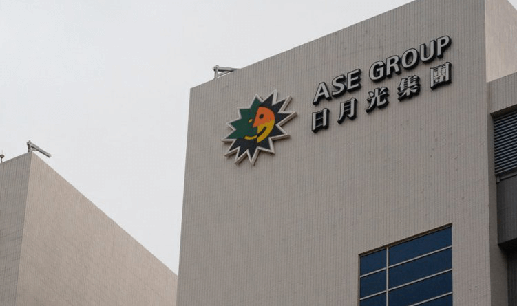
Today, IC packaging and testing service provider Advanced Semiconductor Engineering, Inc. (ASE) held a groundbreaking ceremony for its K13 plant in Kaohsiung. It is expected that the factory will create 2,800 jobs in the future and further create a complete and advanced semiconductor industry cluster.

The report pointed out that the ASE K13 plant has 2 floors underground and 12 floors above ground, with a total area of more than 32,000 square meters. The plant construction is expected to invest 8 billion N.T. dollars. After completion, another 18 billion N.T. dollars will be invested to expand advanced packaging production capacity. The construction of the plant is expected to be completed in 2023, with an estimated annual output value of 500 million U.S. dollars at full load.

ASE stated that the K13 plant will take high-end packaging technology as the core, develop a complete solution for 5G+AIoT smart factories, and achieve a zero-defect, high-efficiency semiconductor packaging and testing 5G smart manufacturing building with high-speed network.

Related

ASE electronic components news K13
UTAC announced the completion of the sale to Wise Road Capital
Previous
Topology releases IC packaging and testing service provider ranking in 20Q2
Next

All Comments (0)

Back
No Comment.

Top Post

Fire broke out at AKM factory in Japan
Mouser Electronics expands to the Philippines with local customer service center
Qualcomm ranked first in the world's top ten IC design companies
Analyze the key factors and prospects of electronic components shortage from the perspective of wafer industry
What is the root cause of the decline of the Japanese semiconductor industry?
ST releases price increase notice

Subscribe SemiMedia

Please check your E-mail to confirm the subscribtion.

Related posts

South Korea weighs $3 billion plan to build new foundry to boost chip ecosystem

South Korea weighs $3 billion plan to build new foundry to boost chip ecosystem

December 12, 2025
0
NXP to shut down ECHO fab as it retreats from 5G RF power market

NXP to shut down ECHO fab as it retreats from 5G RF power market

December 12, 2025
0
Global chip industry enters new AI-driven cycle as market heads toward $1 trillion

Global chip industry enters new AI-driven cycle as market heads toward $1 trillion

December 11, 2025
0
Murata ventures into quantum cryptography to extend semiconductor and components market

Murata ventures into quantum cryptography to extend semiconductor and components market

December 11, 2025
0
3
Copyright © 2017-2025 SemiMedia. Designed by nicetheme.
  • Please set up your first menu at [Admin -> Appearance -> Menus]
  • electronic components news
  • Electronic components supplier
  • Electronic parts supplier
  • Infineon
  • Electronic component news
  • Renesas
  • Vishay
  • STMicroelectronics
  • NXP
  • TDK

SemiMediaEdit

Administrator