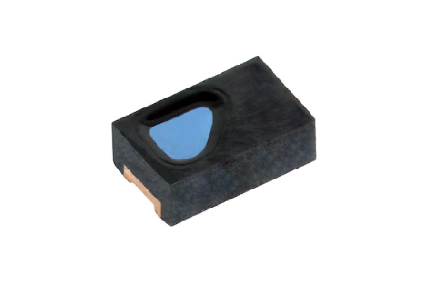
Vishay Intertechnology, Inc. introduced a new 200 V n-channel MOSFET that offers industry-low typical on-resistance of 61 mΩ at 10 V in the 3.3 mm by 3.3 mm thermally enhanced PowerPAK® 1212-8S package, in addition to improved on-resistance times gate charge — a critical figure of merit (FOM) for MOSFETs used in switching applications — of 854 mΩ*nC. Purpose-built to increase power density, the space-saving Vishay Siliconix SiSS94DN is 65 % smaller than devices with similar on-resistance in 6 mm by 5 mm packages.
The typical on-resistance of the TrenchFET® Gen IV power MOSFET released today is 20 % lower than the next best product on the market in a similar package size, and its FOM is 17 % lower than the previous-generation solution. These values result in reduced conduction and switching losses to save energy. With its compact size, the flexible device allows designers to save PCB space by replacing a much larger MOSFET with the same conduction losses, or a similar sized MOSFET with higher conduction losses.
The SiSS94DN is ideal for primary-side switching for isolated DC/DC topologies and synchronous rectification in telecom equipment, computer peripherals, and consumer electronics; LED backlighting for notebooks, LED TVs, vehicles, and vessels; and motor drive control, load switching, and power conversion for GPS, factory automation, and industrial applications.
The device is 100 % RG- and UIS-tested, RoHS-compliant, and halogen-free.
Samples and production quantities of the SiSS94DN are available now, with lead times of 12 weeks. More information please vist https://www.vishay.com/ppg?77350.


All Comments (0)